Integration of electron-beam and optical lithography, for the development of quantum coherent electronics
As the functionalities of proof-of-principle quantum supercon ducting circuits are becoming ever more sophisticated, their integration into larger devices, with complex layouts, has become a milestone for the com munity. Given the vast experience of the semi conductor industry, one could assume that the task of connecting microelectronic lithographic structures is a completely solved problem. However, when dealing with quantum coherent circuits the challenge is quite serious: In contrast to CMOS, where one only needs to worry about galvanic contacts, quantum circuits also need to remain quantum coherent.
At the end of this project, we are happy to report that the main objectives were successfully achieved. We implemented and tested the fabrication of quantum coherent contacts between different lithographic layers. We tested these contacts by integrating them in superconducting microwave resonators, and we mea sured no degradation compared to state-of-the-art coherence. Therefore, we believe our results are directly applicable to current superconducting qubit and resonator designs, allowing a significant increase in their complexity. Our results will also enable to interface superconducting circuits with other me soscopic quantum systems, such as semiconduct ing structures or topological insulators, without losing quantum coherence.
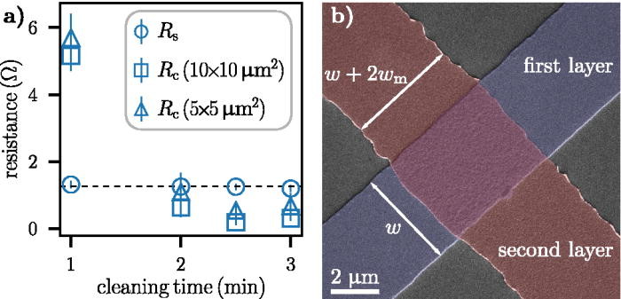
To test the contacting procedure, we decided to use two optical lithography steps. The resulting contacts and the contact resistance are shown in the figure. The procedure was validated by the measurement of state-of-the-art levels of coher ence in quantum resonators fabricated using this method. The method is currently being used in our groups for complex circuit designs. These results have been published in Applied Physics Letters a top-tier peer review journal.

