Towards Massively Parallelized Electrochemical Dip-Pen Nanolithography
Electrochemical Dip-Pen Nanolithography (E-DPN) is a versatile process for creating miniature electronics. Devices can be made from different metals and with high precision. Due to limitations such as area coverage, process duration or wear of the tip, it is, however, only used on laboratory scale. To switch from writing with only one tip to a parallel process with 1D or even 2D tip arrays, may overcome these drawbacks. DPN-specialist Dr. Dr. Michael Hirtz and Dr. Julia Syurik, an expert in Electrochemical Atomic Force Microscopy (E-AFM), got the idea during a traditional "Get-together" part of the YIN meeting und successfully applied for a YIN grant.
In the project, we have proposed to demonstrate the potential for upscaling E-DPN by establishing a parallel E-DPN setup for reproducible writing of metal nanodots for nano-electronics and other applications.
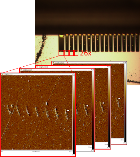
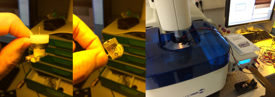
As commercially available DPN systems do not feature a field source and isolated sample and tip holder, a modification of the system was required. In addition, a precise control over the distance between the cantilever and the surface, was not allowed by the standard DPN system due the absence of feedback loop and workarounds had to be found. Therefore, a big part of the project was to find feasible technical solutions and optimizing the designs based on feedback from the experiments until parallel writing could be achieved. The customized E-DNP system was tested by writing of dots and lines of Ni from a 20% aqueous solution of Nickel Chloride-Hexahydrate (NiCl2·6H2O) with varying tip-sample voltage, distance and speed. The best structures were created at 3V and 10nm/sec with the resulting height of about 1.5nm. The shape and the distance between the structures could be well controlled during the process, resulting in significant increase of area coverage without losing the quality.
Such structures with highly defined shape and position are very promising to address such problems as adhesion of Carbon nanotubes (CNTs) when they are made of transition metals (like Ni) or they can serve as photonic nanodots for example for water splitting. The described project has demonstrated the general feasibility of parallel E-DPN and elucidated the needed adjustment to presently available equipment, the research
studies of the Ni nanodots as catalytic centers are ongoing and will be a first step towards application of the new technique.


